Gallium Oxide Materials Science and Engineering MURI (GAME MURI)
β-Ga2O3 possesses transformative potential for power electronic devices, high frequency devices, and deep UV optoelectronics. The Gallium Oxide Materials Science and Engineering (GAME) MURI objective is to develop the basic materials understanding that will enable these applications. Our MURI team is a collaboration between several groups from UCSB, OSU, Cornell and Georgia Tech. The GAME MURI program is comprised of three major themes on Defect Science, Transport and Optical Properties, and Alloys and Interfaces. The target for the project is to provide broad understanding of the β-Ga2O3 material, including the epitaxial growth and material properties and electronic properties, and thus set a stage for both electronic and optoelectronic device applications.
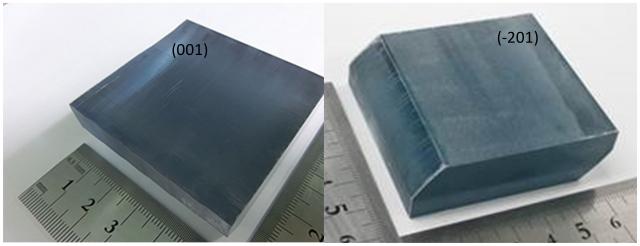
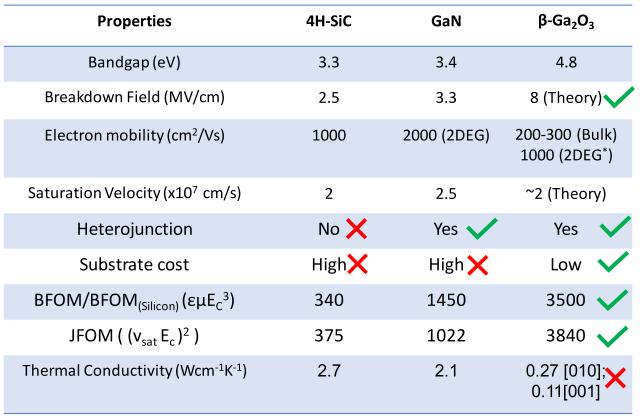
β-Ga2O3 is the largest bandgap (~4.5 eV) semiconductor that can be grown directly from the melt in single crystal form using edge-defined film-fed growth (EFG) and Czochralski growth methods. Commercially available melt-grown β-Ga2O3 wafers can be obtained with crystal surfaces oriented along various directions.The ease of n-type doping with tetravalent cations, and a wide variety of bulk single crystal and epitaxial film growth techniques have triggered worldwide interest in β-Ga2O3. The predicted breakdown electric field (6-8 MV/cm) is higher than that of GaN or SiC (~3 MV/cm), which when combined with electron mobility (predicted ~250-350 cm2/Vs) and electron velocity (predicted ~ 2×107 cm/s) yields amongst the best figures of merit for power electronic and high frequency devices.